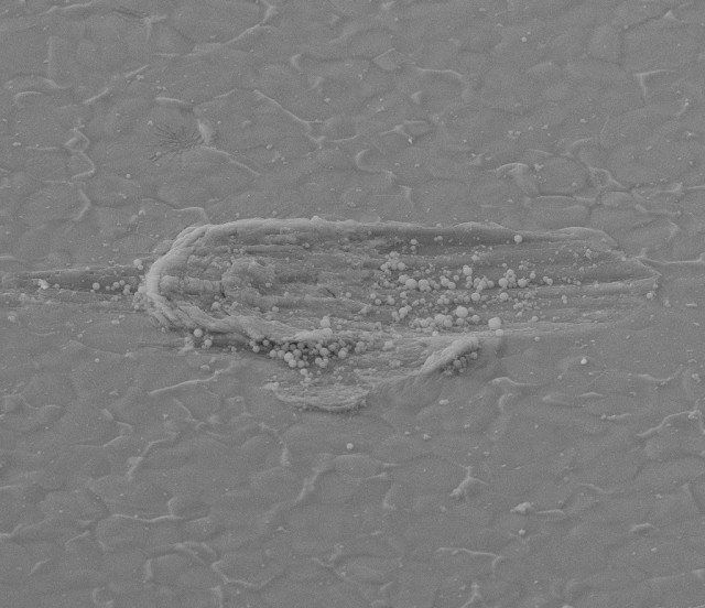
Probe mark....
OK, this will most likely be the first in a series of Scanning Electron Microscope images which may interest some but will probably bore the pants off 99.99% of the Blip population.
Though I would love to hear your thoughts.
Here we go....
I basically sit at a Scanning Electron Microscope (SEM) most days with the aim being either learning about a particular microchip or applying changes to the circuitry within it (editing) using the Focused Ion Beam (FIB) part of my instrument. Today I was mostly performing tests which was quite dull.
When a chip is made, it will be one of potentially thousands on a single wafer of silicon, usually ranging from 150mm to 300mm in diameter. When the wafer goes to be tested to see which chips work and which don't, the wafer gets probed by a very clever and very fast machine. A cluster of tiny metal probes are presented to the wafer and steps across it to ensure every chip gets tested.
What my image shows is the tiny scratch on the chip's test pad which is left by the probe tip.
The field of view of this image is around 35 microns which equates to a 8,000 times magnification of the subject. This would certainly not be visible with the naked eye.
Thanks for listening to me drone on.....
Tone.
557
views
- 1
- 0
Comments
Sign in or get an account to comment.


