
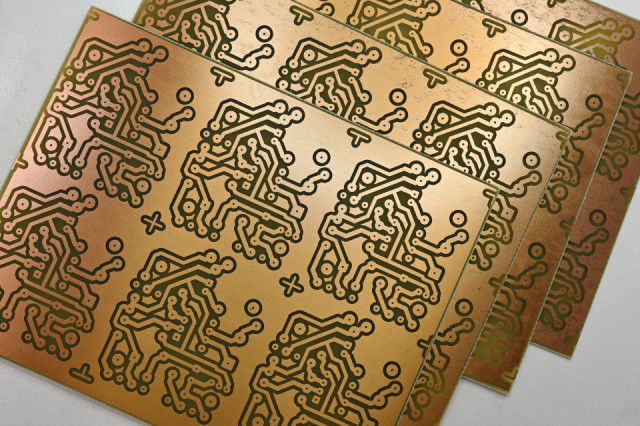
Printed circuit board (PCB) manufacture day. First time in about a year, and despite making a couple of wee test boards, there were a few problems initially. Much better later.
Have been using the same small batch of acid to make several hundred boards for the past five years. Started by decanting the liquid and filtering the sediment from all those previous boards made, and there's possibly another two or three years use still in the remaining acid. In the past they used use about four times my mere 2.5 litres... every year! So huge quantities of chemical waste were generated. Changed the design methodology so that I'm using smaller boards and etching off the minimum amount of copper - just from areas close to the tracks and pads, whilst trying to make it easy for the Students to assemble and solder the components in the circuit. Have also developed all sorts of wee tweaks and features to make it easy for folk to check the boards, like orientating polarised components (ones that have to be connected-up a specific way around) all the same way. That does make it more challenging designing the layouts, but once the design's done (and proven) you can churn out the board, as above.
More to make tomorrow, then a few thousand little holes to be drilled, and finally cut out the individual boards - six to each sheet for the above design.
Extra - usual view over the lower lochan at Inverness Campus this morning.
Comments New comments are not currently accepted on this journal.